Anti-phase domain
An antiphase domain (APD) is a type of planar crystallographic defect in which the atoms within a region of a crystal are configured in the opposite order to those in the perfect lattice system. Throughout the entire APD, atoms sit on the sites typically occupied by atoms of a different species. For example, in an ordered AB alloy, if an A atom occupies the site usually occupied by a B atom, a type of crystallographic point defect called an antisite defect is formed. If an entire region of the crystal is translated such that every atom in a region of the plane of atoms sits on its antisite, an antiphase domain is formed. In other words, an APD is a region formed from antisite defects of a parent lattice. On either side of this domain, the lattice is still perfect, and the boundaries of the domain are referred to as antiphase boundaries.[1] Crucially, crystals on either side of an antiphase boundary are related by a translation, rather than a reflection (a crystal twin) or an inversion (an inversion domain).
Mechanism
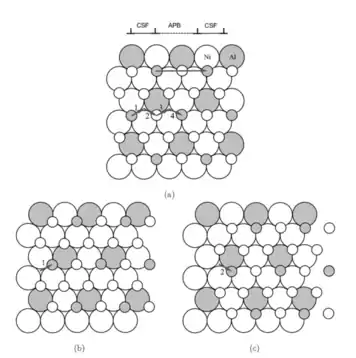
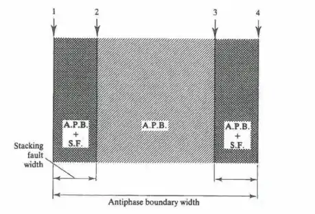
These planar defects are similar to stacking faults in that they are often created through slip of atomic planes and dislocation motion, but the degree of translation varies. In stacking faults, the region of stacking mismatch is bounded by two partial dislocations, and an extended dislocation is formed. For anti-phase domains which only exhibit chemical disorder, the region is bounded by two complex stacking faults, which exhibit both stacking and chemical disorder.[1] Thus, it takes 4 partial dislocations to fully restore the order of the crystal. These can be seen in Figure 1 and 2 below. The width of these regions is determined by the force balance between the like-signed partial dislocations’ repulsion and the regions surface energy. As the anti-phase boundary surface energy increases, the degree of separation between the partial dislocations will decrease to compensate.

Figure 1: This figure depicts two layers of atoms in a Ni3Al crystal, a binary alloy that often exhibits anti-phase boundaries. For visualization purposes, the atoms in the bottom layer are shown as larger than the top layer, but this is not actually the case. The translation of the top layer can be broken down into two steps, indicated by the small arrows 1 and 2. (b) The partial sliding of the top layer by the short vector 1 leads to the formation of a complex stacking fault. (c) The complete sliding of the top layer with the translation magnitude given by a unit lattice translation (1+2), resulting in the formation of an anti-phase boundary. If the top plane slips by two complete lattice spacings (1, 2, 3, and 4), a superdislocation is formed, and this is required for the perfect crystal structure to be restored. It is expected that this superdislocation, consisting of two perfect lattice translations, dissociates into four different partial dislocations with two on each side.[2]

Figure 2: An antiphase boundary created by four partial dislocations (1,2,3,4), surrounded by complex stacking faults. Outside of these shaded regions, the crystal is perfect.[1]
Order Strengthening
Order strengthening brought about from the interaction of dislocations with ordered precipitates, forming anti-phase boundaries as dislocations move throughout the crystal, can lead to significant increases in strength and creep resistance. For this reason, order strengthening is often exploited for high-temperature creep resistant superalloys used in turbine blades.[2]
Antiphase domains carry with them a surface energy penalty when compared to the perfect lattice due to their chemical disorder, and the presence of these boundaries impedes dislocation motion throughout the crystal, leading to increased strength under shear stress. Figure 3 below shows the process of an edge dislocation propagating through an ordered particle. As the dislocation moves throughout the particle, lattice planes are displaced from their equilibrium configuration, and A-A bonds and B-B bonds are formed throughout the slip plane. This forms a higher energy state than when compared to the equilibrium A-B bonding configuration, and the change in energy is called the anti-phase boundary energy (APBE). This can increase the degree of strengthening created from precipitation hardening, making it more difficult for cutting to occur, and instead increasing the likelihood of Orowan bowing around the precipitate.[1]

Figure 3: The process of an edge dislocation moving through an ordered precipitate. In (a), the perfectly ordered particle is shown. In (b), the dislocations has moved through part of the particle. In (c), the dislocation exits the precipitate, leading to an increase in surface energy from increased surface area and a higher-energy bonding configuration.[1]
Order strengthening is often characterized by a ratio of the attractive anti-phase boundary energy (APBE) to the repulsive dislocation energy(Gb): . The degree of order strengthening depends on both this ratio and whether the alloy is in the early or late stages of precipitation. When is low, the trailing dislocation moves far behind the leading dislocations, leading to separate cutting of precipitates as seen in Figure 4a. Alternatively, when is high, the trailing dislocation follows close behind the leading dislocation, leading to common cutting as seen in Figure 4b. During the early stages of precipitation, the increase in shear stress can be expressed as:
for low or
for high where G is the shear modulus, f is the volume fraction of precipitates, r is the radius of the precipitate, and b is the burgers vector of the dislocation.
In the later stages of precipitation, the analogous expressions are:
for low or
for high .[1]

Figure 4: Dislocation motion around precipitates.[1]
Examples from Literature
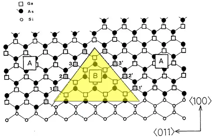
Confusion between inversion domains and antiphase domains is common, even in the published literature, and particularly in the case of GaAs grown on silicon. (Similar defects form in GaN on silicon, where they are correctly identified as inversion domains). An example is illustrated in the diagram below.[3]

Figure 4. Highlighted area showing an inversion domain, incorrectly called an antiphase domain, in GaAs on Si.[4]
The shaded region, B, is an example of an APD. In the figure, GaAs is grown on a misoriented surface of Si (details are not discussed here). The misorientation causes the Ga and As atoms in region B to be on opposite sites compared to the crystal matrix. The presence of the APD results in Ga sites 1, 1’, 2, 2’, 3, 3’ being bonded to Ga atoms in the APD to form an APB.
In mixed oxidation state materials like magnetite, antiphase domains and antiphase domain boundaries can occur as a result of charge-ordering even though there are no changes in atom locations.[4] For example, the reconstructed magnetite (100) surface contains alternating FeII pairs and FeIII pairs in the first subsurface layer.[4] An antiphase domain boundary can form if two subsurface FeII pairs meet when two terraces grow together.[4]
References
- Courtney, Thomas (2000). Mechanical Properties of Materials. McGraw Hill. pp. 203–205.
- Cai, Nix, Wei, William (2016). Imperfections in Crystalline Solids. Cambridge University Press. pp. 575–577.
- Although the journal paper cited below emphasizes self-annihilation of APBs, the picture was taken as an illustration of an APD
- Parkinson, G. S.; Manz, T. A.; Novotny, Z.; Sprunger, P. T.; Kurtz, R. L.; Schmid, M.; Sholl, D. S.; Diebold, U. (2012). "Antiphase domain boundaries at the Fe3O4(001) surface" (PDF). Phys. Rev. B. 85 (19): 195450:1–7. Bibcode:2012PhRvB..85s5450P. doi:10.1103/PhysRevB.85.195450.