Two-dimensional semiconductor
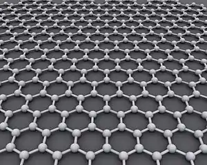
A two-dimensional semiconductor (also known as 2D semiconductor) is a type of natural semiconductor with thicknesses on the atomic scale. Geim and Novoselov et al. initiated the field in 2004 when they reported a new semiconducting material graphene, a flat monolayer of carbon atoms arranged in a 2D honeycomb lattice.,[1] A 2D monolayer semiconductor is significant because it exhibits stronger piezoelectric coupling than traditionally employed bulk forms. This coupling could enable applications.[2] One research focus is on designing nanoelectronic components by the use of graphene as electrical conductor, hexagonal boron nitride as electrical insulator, and a transition metal dichalcogenide as semiconductor.[3][4]
Materials

Graphene
Graphene, consisting of single sheets of carbon atoms, has high electron mobility and high thermal conductivity. One issue regarding graphene is its lack of a band gap, which poses a problem in particular with digital electronics because it is unable to switch off field-effect transistors (FETs).[3] Nanosheets of other group-IV elements (Si, Ge and Sn) present structural and electronic properties similar to graphene.[5]
-side-3D-balls.png.webp)
Hexagonal boron nitride
Monolayer hexagonal boron nitride (h-BN) is an insulator with a high energy gap (5.97 eV).[6] However, it can also function as a semiconductor with enhanced conductivity due to its zigzag sharp edges and vacancies. h-BN is often used as substrate and barrier due to its insulating property. h-BN also has a large thermal conductivity.

Transition metal dichalcogenides
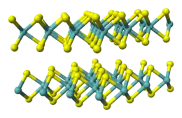
Transition metal dichalcogenide monolayers (TMDs or TMDCs) are a class of two-dimensional materials that have the chemical formula MX2, where M represents transition metals from group VI, V and VI, and X represents a chalcogen such as sulfur, selenium or tellurium.[7] MoS2, MoSe2, MoTe2, WS2 and WSe2 are TMDCs. TMDCs have layered structure with a plane of metal atoms in between two planes of chalcogen atoms as shown in Figure 1. Each layer is bonded strongly in plane, but weakly in interlayers. Therefore, TMDCs can be easily exfoliated into atomically thin layers through various methods. TMDCs show layer-dependent optical and electrical properties. When exfoliated into monolayers, the band gaps of several TMDCs change from indirect to direct,[8] which lead to broad applications in nanoelectronics,[3] optoelectronics,[9][10] and quantum computing [11] .
Synthesis

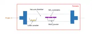
2D semiconductor materials are often synthesized using a chemical vapor deposition (CVD) method. Because CVD can provide large-area, high-quality, and well-controlled layered growth of 2D semiconductor materials, it also allows synthesis of two-dimensional heterojunctions.[12] When building devices by stacking different 2D materials, mechanical exfoliation followed by transferring is often used.[4][7] Other possible synthesis methods include chemical exfoliation, hydrothermal synthesis, and thermal decomposition.
Proposed applications

Some applications include electronic devices,[14] photonic and energy harvesting devices, and flexible and transparent substrates.[3] Other applications include on quantum computing qubit devices[11] solar cells,[15] and flexible electronics.[7]

Quantum computing
Theoretical work has predicted the control of the band edges hybridization on some van der Waals heterostructures via electric fields and proposed its usage in quantum bit devices, considering the ZrSe2/SnSe2 heterobilayer as an example.[11] Further experimental work has confirmed these predictions for the case of the MoS2/WS2 heterobilayer.[16]
Magnetic NEMS
2D layered magnetic materials are attractive building blocks for nanoelectromechanical systems (NEMS): while they share high stiffness and strength and low mass with other 2D materials, they are magnetically active. Among the large class of newly emerged 2D layered magnetic materials, of particular interest is few-layer CrI3, whose magnetic ground state consists of antiferromagnetically coupled ferromagnetic (FM) monolayers with out-of-plane easy axis. The interlayer exchange interaction is relatively weak, a magnetic field on the order of 0.5 T in the out-of-plane (𝒛) direction can induce spin-flip transition in bilayer CrI3. Remarkable phenomena and device concepts based on detecting and controlling the interlayer magnetic state have been recently demonstrated, including spin-filter giant magnetoresistance, magnetic switching by electric field or electrostatic doping, and spin transistors. The coupling between the magnetic and mechanical properties in atomically thin materials, the basis for 2D magnetic NEMS, however, remains elusive although NEMS made of thicker magnetic materials or coated with FM metals have been studied.
References
- Novoselov, K. S. (2004). "Electric Field Effect in Atomically Thin Carbon Films". Science. 306 (5696): 666–669. arXiv:cond-mat/0410550. Bibcode:2004Sci...306..666N. doi:10.1126/science.1102896. ISSN 0036-8075. PMID 15499015.
- Song, Xiufeng; Hu, Jinlian; Zeng, Haibo (2013). "Two-dimensional semiconductors: recent progress and future perspectives". Journal of Materials Chemistry C. 1 (17): 2952. doi:10.1039/C3TC00710C.
- Radisavljevic, B.; Radenovic, A.; Brivio, J.; Giacometti, V.; Kis, A. (2011). "Single-layer MoS2 transistors". Nature Nanotechnology. 6 (3): 147–150. Bibcode:2011NatNa...6..147R. doi:10.1038/nnano.2010.279. PMID 21278752.
- Geim, A. K.; Grigorieva, I. V. (2013). "Van der Waals heterostructures". Nature. 499 (7459): 419–425. arXiv:1307.6718. doi:10.1038/nature12385. ISSN 0028-0836. PMID 23887427.
- Garcia, J. C.; de Lima, D. B.; Assali, L. V. C.; Justo, J. F. (2011). "Group IV graphene- and graphane-like nanosheets". J. Phys. Chem. C. 115 (27): 13242. arXiv:1204.2875. doi:10.1021/jp203657w.
- Dean, C. R.; Young, A. F.; Meric, I.; Lee, C.; Wang, L.; Sorgenfrei, S.; Watanabe, K.; Taniguchi, T.; Kim, P.; Shepard, K. L.; Hone, J. (2010). "Boron nitride substrates for high-quality graphene electronics". Nature Nanotechnology. 5 (10): 722–726. arXiv:1005.4917. Bibcode:2010NatNa...5..722D. doi:10.1038/nnano.2010.172. ISSN 1748-3387. PMID 20729834.
- Wang, Qing Hua; Kalantar-Zadeh, Kourosh; Kis, Andras; Coleman, Jonathan N.; Strano, Michael S. (2012). "Electronics and optoelectronics of two-dimensional transition metal dichalcogenides". Nature Nanotechnology. 7 (11): 699–712. Bibcode:2012NatNa...7..699W. doi:10.1038/nnano.2012.193. ISSN 1748-3387. PMID 23132225.
- Kuc, A.; Zibouche, N.; Heine, T. (2011). "Influence of quantum confinement on the electronic structure of the transition metal sulfideTS2". Physical Review B. 83 (24): 245213. arXiv:1104.3670. Bibcode:2011PhRvB..83x5213K. doi:10.1103/PhysRevB.83.245213. ISSN 1098-0121.
- Wilson, J.A.; Yoffe, A.D. (1969). "The transition metal dichalcogenides discussion and interpretation of the observed optical, electrical and structural properties". Advances in Physics. 18 (73): 193–335. Bibcode:1969AdPhy..18..193W. doi:10.1080/00018736900101307. ISSN 0001-8732.
- Yoffe, A D (1973). "Layer Compounds". Annual Review of Materials Science. 3 (1): 147–170. Bibcode:1973AnRMS...3..147Y. doi:10.1146/annurev.ms.03.080173.001051. ISSN 0084-6600.
- B. Lucatto; et al. (2019). "Charge qubit in van der Waals heterostructures". Physical Review B. 100 (12): 121406. arXiv:1904.10785. doi:10.1103/PhysRevB.100.121406.
- Duan, Xidong; Wang, Chen; Shaw, Jonathan C.; Cheng, Rui; Chen, Yu; Li, Honglai; Wu, Xueping; Tang, Ying; Zhang, Qinling; Pan, Anlian; Jiang, Jianhui; Yu, Ruqing; Huang, Yu; Duan, Xiangfeng (2014). "Lateral epitaxial growth of two-dimensional layered semiconductor heterojunctions". Nature Nanotechnology. 9 (12): 1024–1030. Bibcode:2014NatNa...9.1024D. doi:10.1038/nnano.2014.222. ISSN 1748-3387. PMID 25262331.
- Ong, Zhun-Yong; Bae, Myung-Ho (2019). "Energy dissipation in van der Waals 2D devices". 2D Materials. 6 (3): 032005. arXiv:1904.09752. doi:10.1088/2053-1583/ab20ea.
- "Stanford 2D Device Trends".
- Shanmugam, Mariyappan; Jacobs-Gedrim, Robin; Song, Eui Sang; Yu, Bin (2014). "Two-dimensional layered semiconductor/graphene heterostructures for solar photovoltaic applications". Nanoscale. 6 (21): 12682–12689. Bibcode:2014Nanos...612682S. doi:10.1039/C4NR03334E. ISSN 2040-3364. PMID 25210837.
- Kiemle, Jonas; et al. (2020). "Control of the orbital character of indirect excitons in MoS2/WS2 heterobilayers". Phys. Rev. B. 101 (12): 121404. arXiv:1912.02479. doi:10.1103/PhysRevB.101.121404.